
Dutch deeptech hardware company Morphotonics has secured €40 million ($44.5 million) in an extended funding round to scale its large-area nanoimprint lithography (NIL) equipment and pivot into optical interconnects for AI data centers. Announced on September 22, 2026, the Eindhoven-based company is expanding beyond its core display business—where it manufactures critical waveguides for consumer smart glasses—to help resolve the mounting power and bandwidth bottlenecks inside hyperscale computing clusters.
By adapting the high-speed optical patterning techniques it created for augmented reality (AR) lenses, Morphotonics is betting that light can replace copper wiring inside data centers faster and far more economically than conventional semiconductor methods allow.
€40M War Chest: The Deal and the Backers
The €40 million capital injection is structured as an extended multi-tranche funding round that began with an initial closing in late 2024 and concluded with substantial institutional commitments.
The round includes existing and new high-profile industrial and sovereign investors:
- 3M Ventures (the corporate venture arm of 3M Company)
- Innovation Industries (leading European deeptech VC)
- BOM (Brabant Development Agency)
- Invest-NL (the Dutch national impact investment institution)
- European Innovation Council (EIC) Fund
- European Investment Bank (EIB)
- Ernij Next (Dutch private family office)
Morphotonics has used the multi-stage financing to more than double its operational team, growing from approximately 30 employees in September 2024 to 60 workers today, with targeted stabilization between 70 and 75 personnel as commercial rollouts accelerate.
Nanoimprint Lithography Explained: From Rolls to Wafers
 Photo: ecosistemastartup.com (source)
Traditional semiconductor manufacturing relies heavily on projection photolithography, using ultra-short wavelengths of light and complex mirror arrays to burn patterns into silicon wafers. Morphotonics takes a fundamentally different mechanical approach known as Roll-to-Plate (R2P) Nanoimprint Lithography.
Instead of exposing circuits using multi-million-dollar optical scanners, Morphotonics uses precision-engineered flexible polymer stamps mounted on rolling drums. As the roller glides smoothly across large glass sheets, polymers, or semiconductor wafers, it stamps intricate nanometer- and micrometer-scale optical structures directly into photo-curable liquid resists. Ultraviolet light cures the resin instantly upon contact, transferring trillions of precise optical prisms, lenses, or diffraction gratings across surfaces exceeding one square meter.
This continuous mechanical rolling process bypasses two major hurdles of rigid-stamp lithography: air bubbles and uneven mechanical pressure. As a result, Morphotonics achieves production yields of 90% to 95%, turning optical components that were once notoriously expensive lab prototypes into commercially mass-producible components.
Equipment Lineup: R&D to High-Volume Foundry
Morphotonics provides complete production platforms spanning experimental development to automated mass production:
| Platform | Primary Use Case | Substrate Formats | Target Throughput / Capacity |
|---|---|---|---|
| Portis Series | Laboratory R&D and process testing | Wafers and small glass plates | Low-volume, rapid formulation runs |
| Aurora Series | Automated display and surface manufacturing | Large glass sheets (up to Gen 5 sizes) | Industrial panel line volume |
| Cypris Series (X600) | High-volume AR waveguide fabrication | Multi-wafer and panel-scale substrates | Over 6,000,000 waveguides/year per line |
The flagship Cypris production line is engineered specifically to break the bottleneck holding back the consumer AR industry. Commercial customer deliveries of the Cypris platform are scheduled to commence in early 2027.
The Leap into Data Centers: Routing AI with Photons
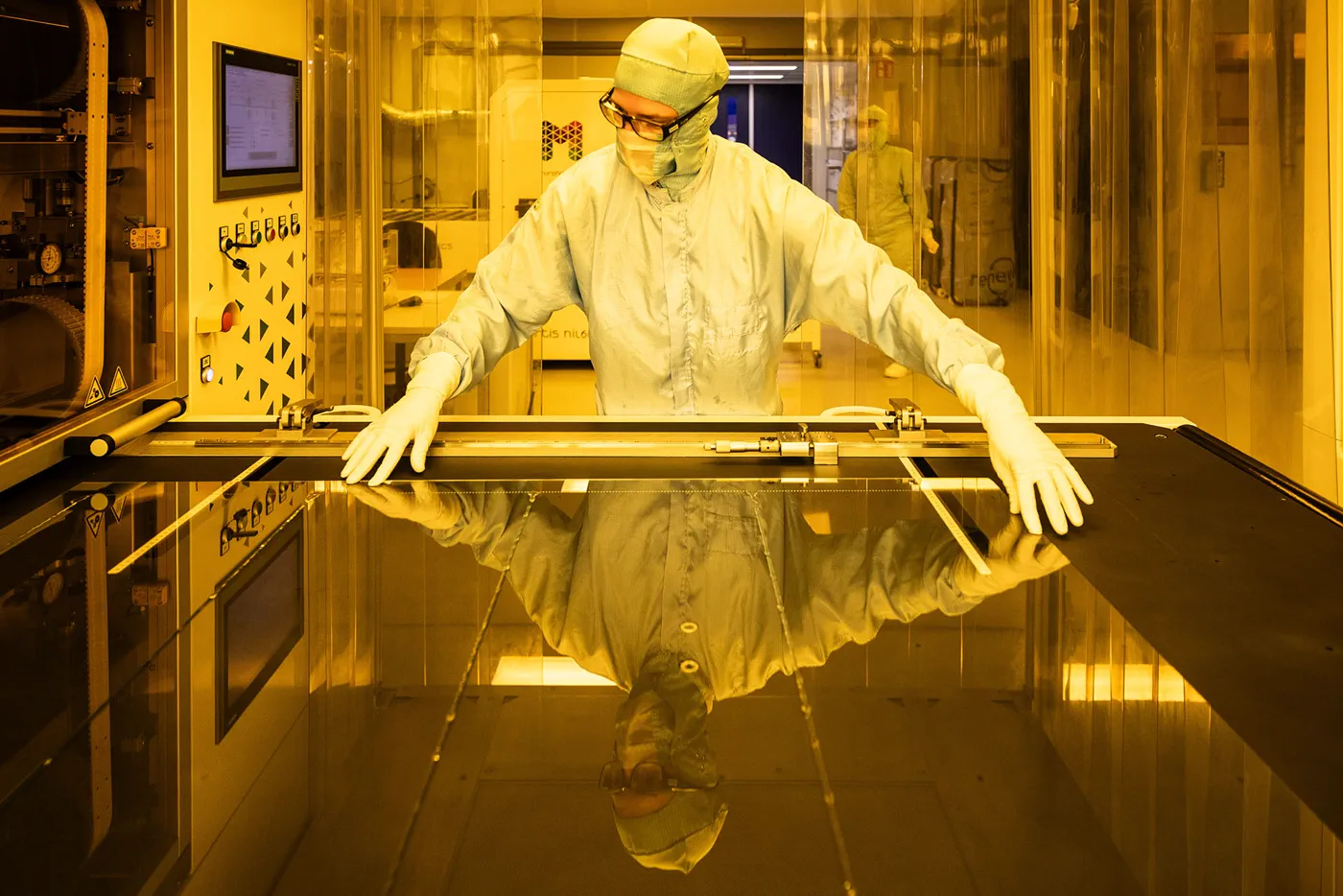 Photo: morphotonics.com (source)
The headline shift funded by this €40 million round is Morphotonics' entry into integrated optics and co-packaged optics (CPO) for data centers.
Modern artificial intelligence clusters require thousands of GPUs communicating in parallel. When data moves between compute nodes over traditional copper cables, electrical resistance generates extreme heat and causes signal degradation, running directly into physical bandwidth walls. Moving signals with light (photons) rather than electricity (electrons) cuts energy losses dramatically.
However, optical interconnects, micro-lenses, and photonic packaging require nanometer-precise optical interfaces to align fibers and chips. By repurposing its roll-to-plate stamping machines, Morphotonics can manufacture microscopic waveguides and optical coupling components on large substrates with extreme repeatability. Instead of treating optical routing as an expensive semiconductor step, Morphotonics allows hyperscalers to mass-produce optical interposers and data-routing surfaces at commercial scale.
From Philips Roots to ASML Neighbor: The Eindhoven Advantage
Morphotonics was founded in 2014 in Veldhoven, right in the heart of the Netherlands' Brainport Eindhoven tech cluster. The engineering heritage of the company traces back to technology originally pioneered by Royal Philips for stamping microscopic tracks on compact discs and DVDs.
Headquartered in the exact same municipality as lithography giant ASML, Morphotonics actively leverages the region’s dense precision-engineering supplier base. Chief Executive Officer Hugo da Silva, who joined the helm in late 2024 after leadership tenures at DSM and Dow Corning, emphasized that tapping into ASML’s regional ecosystem and supply chain partners provides Morphotonics an unparalleled edge in mechatronics, motion control, and nano-precision assembly.
How Morphotonics Compares to Industry Alternatives
 Photo: startupintros.com (source)
| Technology / Approach | Primary Players | Advantages | Disadvantages / Limitations |
|---|---|---|---|
| Roll-to-Plate NIL (Morphotonics) | Morphotonics | Large-area panel processing, high throughput, 90%+ yields, lower machine capex | Dedicated primarily to optics/waveguides, not sub-nanometer logic transistors |
| Projection Photolithography | ASML, Nikon, Canon | Extreme nanoscale sub-3nm resolution for high-performance silicon | Astronomical equipment cost (€100M+ per scanner), rigid silicon wafer size limits |
| Wafer-Level Nanoimprinting | Canon, EV Group (EVG) | High precision for semiconductor-scale packaging | Limited to 200mm–300mm rigid circular wafers; high tooling and die wear costs |
| Direct Laser Writing / E-Beam | Heidelberg Instruments, Raith | Zero-mask flexible prototyping | Impractically slow throughput for high-volume commercial hardware |
Industry Reactions and Real-World Hardware Footprint
Morphotonics' footprint is already embedded in high-profile consumer hardware. The company’s nanoimprinted waveguides are currently used in smart glasses such as the Meta Ray-Ban Display, Even Reality G1, and devices from Magic Leap, in addition to high-end automotive privacy displays.
"3M is excited about our investment in Morphotonics and the potential collaboration opportunity between our companies," said Mark Copman, senior vice president of 3M New Growth Ventures. "Our investment demonstrates 3M's dedication to enabling innovative technology that can drive advancements in consumer electronics."
"At Morphotonics, we are committed to helping customers unlock the full potential of large-area NIL technology," stated CEO Hugo da Silva, highlighting the company’s recent launches of its Global Lab-to-Fab network and manufacturing partnerships with firms like Moveon Technologies in Singapore to scale production lines across the Asia-Pacific region.
What It Means for Smart Glasses and Cloud Hyperscalers
For consumer electronics makers, the industrialization of roll-to-plate lithography removes the single most stubborn hurdle to consumer AR: waveguide cost. While early augmented reality headsets carried price tags in the thousands of dollars partly due to poor waveguide yields, high-throughput panel stamping paves the way toward lightweight, sub-$500 prescription-ready smart glasses.
For cloud operators and data center infrastructure builders, Morphotonics provides a practical roadmap to co-packaged optics. Stamping optical wave-guiding features onto motherboards and interposers will allow AI cluster operators to replace high-power copper traces with light, slashing the megawatts required to shuttle weights across distributed computing nodes.
What Happens Next
Morphotonics faces critical execution milestones heading into 2027:
- Cypris Commercial Deployments: Delivering the initial batch of Cypris X600 high-volume systems to manufacturing partners in Taiwan, South Korea, China, and the United States in early 2027.
- Data Center Prototyping: Validating its first dedicated photonic interconnect tools alongside semiconductor packaging foundries.
- Supply Chain Scaling: Stabilizing its global workforce at 70 to 75 specialists while expanding cleanroom footprint and regional technical hubs.
Frequently Asked Questions
What is Morphotonics and what does it make?
Morphotonics is a Dutch deeptech manufacturing equipment maker that builds Roll-to-Plate Nanoimprint Lithography machines. Its systems stamp microscopic and nanoscale optical features onto large glass and polymer sheets for augmented reality glasses, 3D screens, automotive displays, and data centers.
Who invested in Morphotonics' €40M round?
The €40 million round was supported by 3M Ventures, Innovation Industries, BOM (Brabant Development Agency), Invest-NL, the European Innovation Council (EIC) Fund, the European Investment Bank (EIB), and Dutch family office Ernij Next.
How does roll-to-plate nanoimprint differ from ASML lithography?
While ASML builds optical projection scanners that etch microscopic electronic circuits onto silicon chips using ultraviolet light, Morphotonics mechanically rolls flexible textured stamps directly into resin over large sheets of glass. It specializes in optics, waveguides, and photonic structures rather than silicon transistor logic.
Why is display technology relevant to AI data centers?
Both smart glasses displays and optical data centers rely on waveguides—microscopic channels that control and route light beams. In AI data centers, replacing copper electrical cables with optical waveguides dramatically reduces latency and power consumption between interconnected GPUs.
When will Morphotonics' high-capacity Cypris machine ship?
The company's Cypris manufacturing platform, capable of outputting over 6 million AR waveguides per line each year, is scheduled to begin commercial shipments in early 2027.